LIVE EVENT
GCN Investor Conference in Newport Beach, CA
MARCH 25 · NEWPORT BEACH, CA

LIVE EVENT



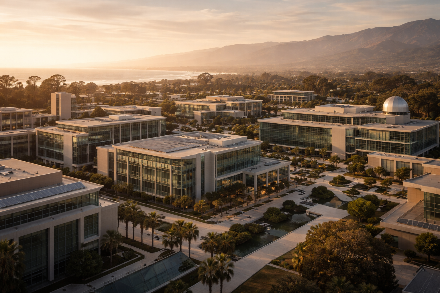
A campus with world-leading materials science, and the research base behind the blue LED.
UC Santa Barbara's materials department is among the strongest anywhere, and its faculty have been recognised at the highest level — the Nobel-recognised work on efficient blue light-emitting diodes was carried out by a professor at the university.
Its strengths in compound semiconductors, photonics, and theoretical physics are disproportionate to the campus's modest size.
Santa Barbara has a small but technically serious cluster, often called Silicon Beach's northern end, focused on semiconductors, photonics, and software.
Several large semiconductor and networking companies in the region trace their origins to university research or faculty founders.
Company formation concentrates in compound semiconductors, photonics, optical networking, and specialised materials.
The campus punches far above its weight in hard technology relative to universities several times its size.
Local capital is limited, but semiconductor and photonics companies attract strategic investors from the global industry.
Los Angeles and Bay Area venture funds participate in software and later-stage rounds.
GCN’s global network includes millions of startups and founders and a broad community of investors, creating opportunities to discover potential connections across university communities.

.webp)
.png)


.png)